
Product Details
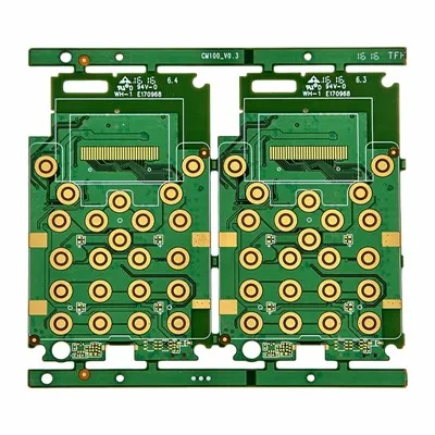
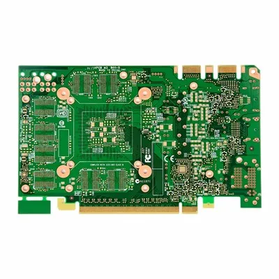
Multilayer PCB consists of two or more conductive copper layers separated by dielectric materials and laminated together, interconnected by plated through-holes, buried vias or blind vias. Compared with single-sided and double-sided PCBs, multilayer PCBs greatly expand routing capacity, improve electromagnetic interference shielding and support complex high-speed circuit designs. They are widely adopted in industrial equipment, computing hardware, communication devices, automotive electronics and consumer products. Stack-up configuration, layer count, material grade and via structure directly affect performance, manufacturability and total cost. Engineers and buyers should define layer count and stack-up based on signal integrity requirements, routing demands and budget constraints, avoiding over-specification that drives unnecessary cost increases.

Project Requires Multilayer PCB
Many purchasing teams receive requests for 4-layer, 6-layer or even 12-layer boards without fully understanding why those layer counts were selected.
In practice, the decision should be based on design requirements rather than assumptions.
A multilayer PCB is usually recommended when a product requires:
- High component density
- Controlled impedance routing
- Multiple power and ground planes
- High-speed signal transmission
- Compact board dimensions
- Reduced EMI and noise
For example, a simple industrial controller may function perfectly on a 2-layer PCB, while a networking device containing processors, memory modules and communication interfaces may require 6 or 8 layers to maintain signal integrity.
Choosing excessive layer counts can increase manufacturing costs unnecessarily, while choosing too few layers may lead to design compromises and performance issues.

Comparing 2-Layer and Multilayer PCB Designs
One common question from buyers is whether upgrading from a 2-layer PCB to a multilayer design is worth the additional investment.
The answer depends on the application's performance requirements.
|
Item |
2-Layer PCB |
Multilayer PCB |
|
Routing Space |
Limited |
High |
|
Signal Integrity |
Basic |
Excellent |
|
EMI Performance |
Moderate |
Better |
|
Board Size |
Larger |
Smaller |
|
Manufacturing Cost |
Lower |
Higher |
|
Design Complexity |
Simple |
Advanced |
|
Suitable for High-Speed Circuits |
Limited |
Yes |
While multilayer PCBs generally cost more to manufacture, they often reduce overall system costs by allowing smaller product dimensions and eliminating design workarounds.
Many compact electronic products would not be feasible without multilayer structures.
Manufacturing Challenges Buyers Should Understand
- Not all PCB manufacturers offer the same multilayer capabilities.
- As layer counts increase, manufacturing complexity rises significantly.
- Several critical processes determine final product quality.
Layer Registration Accuracy
All conductive layers must align precisely during lamination. Even minor registration errors can affect electrical performance and drilling accuracy.
Lamination Control
Multilayer boards undergo high-pressure lamination processes. Improper process control can result in delamination, warpage or reliability issues.
Hole Wall Reliability
Plated through holes connect internal layers. Consistent plating thickness is essential for long-term electrical reliability.
Impedance Control
For communication, networking and high-speed electronic products, impedance consistency is often critical to signal performance.
When evaluating suppliers, buyers should verify whether these capabilities have been proven in actual production rather than relying solely on marketing materials.
Typical Manufacturing Capabilities
The required capability depends on product complexity, but common multilayer PCB specifications include:
|
Specification |
Typical Capability |
|
Layer Count |
4–30 Layers |
|
Board Thickness |
0.4–6.0 mm |
|
Copper Weight |
0.5–6 oz |
|
Surface Finish |
ENIG, OSP, HASL |
|
Minimum Hole Size |
Advanced mechanical drilling |
|
Controlled Impedance |
Available |
|
Blind/Buried Via |
Optional |
Not every project requires advanced specifications. Selecting the right capability level helps control costs while maintaining product performance.
Lead Time Considerations
Lead time is often overlooked during supplier selection.
Compared with standard double-sided boards, multilayer PCB production typically requires additional manufacturing steps, including:
- Inner layer imaging
- Layer alignment
- Lamination
- X-ray registration verification
- Additional quality inspections
As layer count increases, production cycles generally become longer.
Prototype orders may require different lead times than volume production, so early communication with the supplier is important for project planning.
Buyers who involve PCB manufacturers during the design phase often avoid delays caused by manufacturability issues discovered later in production.
Quality Control and Reliability Verification
For industrial, automotive and medical applications, reliability is often more important than achieving the lowest unit cost.
A robust quality system should include:
- Automated Optical Inspection (AOI)
- Electrical testing
- X-ray verification
- Cross-section analysis
- Solderability testing
- Dimensional inspection
These inspections help ensure that internal structures meet design requirements before products move to assembly.
For critical applications, reliability validation may also include thermal cycling and environmental testing to verify long-term performance.
Reduce Purchasing Risk
When sourcing multilayer PCBs, many purchasing problems originate from insufficient technical review rather than manufacturing defects.
To reduce project risk, buyers should verify:
- Layer stack-up design
- Material specifications
- Impedance requirements
- Surface finish selection
- Reliability expectations
Production volume forecasts
Early engineering discussions often identify potential issues before manufacturing begins.
This approach can prevent costly redesigns, qualification delays and unexpected production interruptions.
FAQ
How many layers can a multilayer PCB have?
Commercial multilayer PCBs typically range from 4 to more than 30 layers depending on the application and manufacturing capability.
Does a higher layer count always mean better performance?
No. The optimal layer count depends on routing requirements, signal integrity needs and cost considerations.
Are multilayer PCBs more expensive than double-sided boards?
Yes, because additional materials and manufacturing processes are required. However, they can reduce overall system costs by enabling smaller and more efficient designs.
What industries commonly use multilayer PCBs?
Industrial automation, telecommunications, medical devices, automotive electronics, aerospace systems and consumer electronics all rely heavily on multilayer PCB technology.
Hot Tags: multilayer pcb, China multilayer pcb manufacturers, suppliers, factory, rigid printed circuit board, rigid rigid and flexible pcb