
Product Details
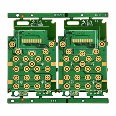
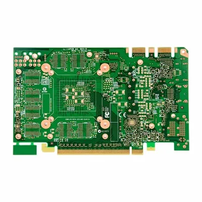
HDI (High-Density Interconnect) PCB is an advanced multilayer circuit board built with laser microvias, blind/buried vias, fine traces and sequential lamination structures. Compared with conventional multilayer PCBs, it delivers much higher wiring density within limited board space, supporting component miniaturization and high-speed signal transmission. Widely adopted in smartphones, medical equipment, automotive electronics, industrial controllers and communication hardware, HDI helps engineers integrate more functions without enlarging board dimensions. Nevertheless, HDI selection should not merely pursue advanced specifications. Procurement and engineering teams need to balance actual design demands, manufacturing capacity and cost factors to make practical sourcing decisions

Limitations of Traditional Multilayer PCBs
Many projects begin with a conventional 4-layer or 6-layer PCB design. As component density increases, engineers often encounter routing challenges that cannot be solved simply by adding more layers.
Common design issues include:
- Insufficient routing channels
- Large component counts
- Fine-pitch BGA packages
- High-speed signal requirements
- Board size restrictions
- Connector density limitations
Increasing board dimensions may not be possible due to product size constraints. Adding additional layers can increase costs while still failing to provide enough routing space.
HDI technology addresses these challenges by creating additional routing opportunities through microvias and finer conductor geometries.

Understanding HDI PCB Structures
Unlike conventional multilayer boards that rely primarily on through-hole vias, HDI PCBs utilize advanced interconnection methods.
Typical HDI features include:
Microvias
Microvias are significantly smaller than standard drilled vias and allow more efficient use of available board space.
01
Blind Vias
Blind vias connect outer layers to internal layers without passing through the entire board.
02
Buried Vias
Buried vias connect internal layers while remaining completely hidden inside the PCB structure.
03
Fine Line Routing
Smaller conductor widths and spacing enable greater circuit density.
04
Sequential Lamination
Multiple lamination cycles create complex interconnection structures that support advanced electronic designs.
These technologies allow designers to place more circuits into smaller areas while maintaining signal integrity.
05
Criteria for HDI PCB Technology Adoption
Not every electronic product benefits from HDI construction.
In some cases, a standard multilayer PCB remains the most cost-effective solution.
HDI is commonly recommended when products contain:
- Fine-pitch BGAs
- High pin-count processors
- Compact mechanical layouts
- High-speed communication interfaces
- Multiple memory devices
- Space-constrained assemblies
- Examples include:
- Smartphones
- Tablets
- Medical monitoring devices
- Automotive control units
- Industrial handheld equipment
- Communication modules
If a design can be routed efficiently using conventional multilayer technology, HDI may not provide sufficient value to justify the additional cost.
Manufacturing Challenges in HDI Production
HDI manufacturing requires significantly tighter process control than standard PCB fabrication.
Several critical processes directly influence product quality.
Laser Drilling Accuracy
Microvias are typically produced using laser drilling systems. Precision is essential to ensure reliable interconnections.
Layer Alignment
As conductor spacing decreases, registration tolerances become increasingly important.
.
Via Reliability
Microvias must maintain electrical integrity throughout thermal cycling and product operation.
Copper Plating Consistency
Uniform copper deposition helps ensure reliable connections within small via structures.
Sequential Lamination Control
Multiple lamination cycles increase manufacturing complexity and require strict process monitoring.
Because of these challenges, not all PCB manufacturers offer advanced HDI capability.
Cost Drivers Buyers Should Understand
HDI boards are generally more expensive than conventional multilayer PCBs.
However, the cost increase is often related to manufacturing complexity rather than raw material consumption.
Key cost factors include:
|
Cost Factor |
Impact on Pricing |
|
Microvia Count |
High |
|
Sequential Lamination Cycles |
High |
|
Layer Count |
Medium to High |
|
Fine Line Requirements |
High |
|
Material Selection |
Medium |
|
Yield Management |
High |
Buyers should evaluate total system cost rather than focusing exclusively on PCB pricing.
In many cases, HDI technology reduces overall product size, assembly complexity and enclosure costs.
Quality and Reliability Considerations
Because HDI structures contain smaller features and more complex interconnections, reliability validation is especially important.
Common quality control procedures include:
- Automated Optical Inspection (AOI)
- X-ray Inspection
- Microsection Analysis
- Electrical Testing
- Registration Verification
- Thermal Reliability Testing
For products used in automotive, industrial or medical environments, reliability testing often becomes a critical part of supplier qualification.
A low-cost HDI board that fails reliability testing can create significantly higher downstream costs than a properly manufactured product.
Future Growth of HDI Technology
Several market trends continue driving HDI adoption:
- Artificial Intelligence hardware
- 5G communication equipment
- Automotive electronics
- Medical devices
- Industrial IoT systems
- Consumer electronics miniaturization
As component packages become smaller and performance requirements continue increasing, HDI PCB technology will remain a key solution for achieving compact, high-performance electronic designs.
Manufacturers that invest in advanced HDI capabilities will be better positioned to support next-generation electronic products across multiple industries.
FAQ
What does HDI stand for?
HDI stands for High Density Interconnect, a PCB technology that uses microvias, fine traces and advanced layer structures to achieve higher circuit density.
Are HDI PCBs always better than standard multilayer boards?
Not necessarily. HDI is most beneficial when space constraints, component density or high-speed signal requirements make conventional designs difficult to implement.
What industries commonly use HDI PCBs?
Consumer electronics, automotive electronics, medical devices, industrial control systems and communication equipment frequently use HDI technology.
Why are HDI PCBs more expensive?
Additional manufacturing processes such as laser drilling, sequential lamination and advanced inspection increase production complexity and cost.
Hot Tags: hdi pcb, China hdi pcb manufacturers, suppliers, factory, rigid printed circuit board, rigid rigid and flexible pcb