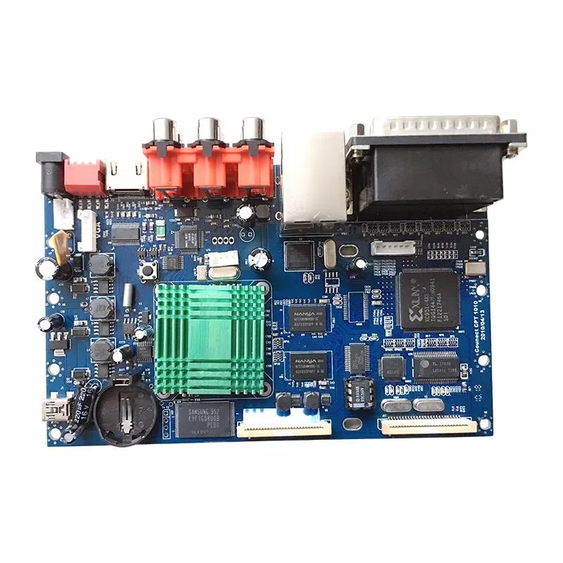
BGA components are widely used in communication equipment, industrial control boards, medical electronics, automotive modules, IoT gateways, embedded systems, computing modules, consumer electronics, and other high-density electronic products. Compared with standard leaded components, BGA packages allow more I/O connections in a smaller space, making them suitable for compact and high-performance PCB designs.
Our BGA PCB Assembly Service is designed for customers who need reliable assembly support for boards with BGA, QFN, LGA, fine-pitch ICs, and other advanced packages. For customers, the main concern is not only whether the BGA component can be placed on the PCB. They want to know whether the solder balls can form reliable joints, whether hidden soldering defects can be inspected, whether the reflow profile is suitable, whether the PCB design is manufacturable, and whether the same process can be repeated in future batches.
BGA assembly requires more careful process control than standard SMT. A defect under the chip cannot be seen by normal visual inspection. Problems such as insufficient solder, bridging, voids, poor wetting, cold joints, component shift, or PCB warpage may cause open circuits, short circuits, unstable function, or intermittent failures. That is why BGA projects require accurate placement, controlled solder paste printing, proper reflow soldering, X-ray inspection, and engineering review before production.
Solving Hidden Solder Joint, Design, and Process Risks
The biggest customer pain point in BGA assembly is hidden solder joint reliability. Since the solder balls are located under the component body, ordinary visual inspection cannot directly confirm soldering quality. A board may look perfect from the outside but still have hidden defects under the BGA package. These defects may only appear during electrical testing, functional testing, temperature changes, vibration, or long-term operation.
BGA soldering quality depends on several factors. The PCB pad design must match the component footprint. The solder mask opening must be suitable. The solder paste volume must be controlled. The placement position must be accurate. The reflow profile must allow proper solder melting without overheating the component or the PCB. The board must also remain flat enough during reflow to avoid poor contact or solder joint separation.
Many BGA problems begin at the design stage. Customers may face issues such as incorrect footprint, unsuitable pad size, poor via-in-pad design, missing test points, improper solder mask design, surface finish problems, or PCB warpage risk. These issues can make assembly more difficult and increase the chance of soldering failure.
A proper DFM review before production can help reduce these risks. The review may include BGA footprint checking, pad design review, solder mask opening assessment, surface finish review, via-in-pad consideration, board thickness and warpage risk review, panelization suggestion, and test point accessibility. This helps customers improve assembly success before boards enter production.
|
Project Area |
Customer Pain Point |
Assembly Focus |
|
BGA Footprint |
Pad size or footprint may not match the component |
Review footprint and pad design before production |
|
Solder Paste Printing |
Too much or too little solder may cause defects |
Control stencil design and solder paste volume |
|
Placement Accuracy |
Component shift may create open or short circuits |
Use accurate placement and process control |
|
Reflow Soldering |
Wrong profile may cause cold joints or overheating |
Control preheat, peak temperature, and cooling |
|
PCB Warpage |
Board deformation may affect solder joint contact |
Review board structure and reflow risk |
|
Hidden Defects |
Solder joints cannot be checked visually |
Use X-ray inspection when required |
|
Batch Production |
Sample quality may not repeat in mass production |
Maintain process records and inspection standards |
A reliable BGA PCBA Manufacturing process should not only complete component placement. It should help customers identify design risks, control soldering conditions, inspect hidden joints, and maintain repeatable quality from prototype to mass production.
BGA Soldering Quality Control
BGA soldering quality is closely related to process stability. Solder paste printing must be controlled to avoid insufficient solder, solder bridging, or uneven solder volume. Placement accuracy is also important because even slight misalignment may affect solder ball connection. Reflow soldering must be carefully managed because the temperature profile determines whether solder balls melt and form reliable joints.
The reflow process should consider PCB thickness, component size, solder paste type, board surface finish, thermal mass, and component sensitivity. If the temperature is too low, solder joints may not form properly. If the temperature is too high, the component or PCB may be damaged. If cooling is not controlled, solder joint stress may increase.
For BGA projects, process control should be planned before production instead of corrected after defects appear. This is especially important for fine-pitch BGA, large BGA packages, high-density multilayer boards, and products that require long-term reliability.
X-ray Inspection for Hidden Solder Joints
X-ray inspection is one of the most important quality control steps for BGA assembly. Since BGA solder joints are hidden under the package, X-ray helps check solder ball alignment, bridging, voids, insufficient solder, and other hidden soldering risks.
For prototype projects, X-ray inspection can help customers confirm whether the first build is suitable for functional testing. For small-batch and mass production, X-ray inspection can help monitor process stability and reduce the risk of hidden defects reaching the customer.
X-ray inspection is also useful for other bottom-terminated components such as QFN, LGA, and some power packages. It gives customers more confidence when normal visual inspection is not enough.
Improving Rework Control, Testing Confidence, and Batch Consistency
BGA rework is another major customer concern. Because BGA components are more difficult to remove and replace than standard SMT parts, rework must be handled carefully. Poor rework may damage PCB pads, affect nearby components, overheat the board, or reduce reliability. For prototype projects, BGA rework capability can help reduce sample waste and development delays if a component needs to be replaced or repaired.
BGA rework may include controlled heating, component removal, pad cleaning, solder preparation, accurate replacement, reflow, and post-rework inspection. After rework, X-ray inspection is recommended to confirm the solder joint condition. Although rework can be helpful, the best approach is still to reduce defects through proper DFM review, accurate placement, and stable reflow control.
Testing is also important. X-ray can check hidden soldering quality, but functional testing is still needed to confirm whether the assembled board works according to customer requirements. Depending on the product, testing may include electrical checks, firmware programming, communication testing, power-on testing, or complete functional testing.
|
Inspection / Testing Item |
Purpose |
Customer Benefit |
|
Incoming Inspection |
Checks PCB and component condition before assembly |
Reduces material-related defects |
|
Solder Paste Inspection |
Checks paste printing quality before placement |
Reduces solder volume problems |
|
AOI Inspection |
Detects visible defects around other SMT components |
Improves overall assembly accuracy |
|
X-ray Inspection |
Checks hidden solder joints under BGA, QFN, and LGA packages |
Reduces hidden soldering risks |
|
Electrical Check |
Detects open circuits, short circuits, and basic connection issues |
Helps identify obvious failures |
|
Functional Testing |
Verifies whether the board works as required |
Confirms real product performance |
|
BGA Rework Inspection |
Checks repaired or replaced BGA components |
Reduces post-rework uncertainty |
|
Final Visual Inspection |
Checks labels, connectors, cleanliness, and packaging |
Reduces shipment and handling risks |
Fine-Pitch and High-Density BGA Assembly
Many modern electronics use fine-pitch BGA packages to save space and increase functionality. These projects often require multilayer PCBs, dense routing, small pads, tight spacing, and high component density. Assembly becomes more challenging because the process window is smaller.
For fine-pitch BGA, pad design, solder mask accuracy, stencil thickness, paste control, placement precision, and reflow stability are all important. If the process is not controlled well, defects may occur more easily. This is why early DFM review and proper inspection are strongly recommended for high-density boards.
Our BGA Assembly Services can support prototype, low-volume, and mass production projects that require careful process planning and inspection. Whether the board is used for industrial control, IoT gateways, communication equipment, medical electronics, automotive electronics, or embedded computing modules, the assembly process should match the product's reliability requirements.

Application Areas
BGA assembly is commonly used in high-performance and high-density electronic products. Communication equipment often requires stable signal transmission and high pin count components. Industrial control boards need long-term reliability and consistent soldering quality. Medical electronics may require inspection records and stable function. Automotive electronics may need strong solder joint reliability under vibration and temperature changes. IoT gateways and embedded systems often use compact layouts with BGA, QFN, and fine-pitch ICs.
Consumer electronics and computing modules also benefit from BGA packaging because it allows compact design and higher functionality. However, these advantages also require better process control and inspection to reduce hidden soldering risks.

Prototype to Mass Production Support
Many BGA projects begin with prototypes. During the prototype stage, customers usually focus on confirming footprint design, soldering quality, X-ray results, firmware operation, and functional performance. After approval, the project may move into small-batch production, pilot runs, or mass production.
To support this transition, approved BOM versions, BGA component specifications, reflow process notes, X-ray inspection standards, testing methods, and rework records should be documented clearly. If a soldering issue is found during the prototype stage, the cause should be reviewed before the next build. If the project moves into mass production, process consistency becomes critical.
For customers, stable batch production is important because BGA defects may be difficult to detect without proper inspection. Clear process control and quality records help reduce repeat problems and improve long-term reliability.

Quality Control and Final Delivery
Quality control for BGA assembly should begin before production. File review, BOM checking, PCB surface finish confirmation, stencil planning, solder paste control, placement accuracy, reflow profile control, X-ray inspection, functional testing, and final packaging all affect final quality.
For BGA projects, packaging and handling should also be controlled carefully. Components may be moisture-sensitive, and boards should be protected from contamination, bending, or damage during shipment. Proper final inspection and packaging help ensure the assembled boards arrive ready for customer testing or product integration.
The goal is to deliver assembled boards that are not only completed, but also reliable enough for real application testing and future production.
FAQ
Q1: What is BGA PCB assembly?
BGA PCB assembly is the process of placing and soldering ball grid array components onto a PCB. Because the solder balls are located under the component, BGA assembly requires accurate placement, controlled reflow soldering, and X-ray inspection when needed.
Q2: Why is X-ray inspection important for BGA?
BGA solder joints cannot be checked by normal visual inspection. X-ray inspection helps detect hidden defects such as bridging, voids, insufficient solder, poor alignment, or other soldering risks under the package. This helps reduce uncertainty before testing or shipment.
Q3: Can you support fine-pitch BGA assembly?
Yes. Fine-pitch BGA assembly can be supported, but it requires careful DFM review, accurate solder paste printing, precise placement, controlled reflow, and proper inspection. Customers should provide complete Gerber files, BOM, placement data, and component information for review.
Q4: What causes BGA soldering defects?
Common causes include poor pad design, unsuitable solder mask opening, unstable solder paste volume, placement offset, incorrect reflow profile, PCB warpage, surface finish problems, moisture sensitivity, or component condition issues. Early review and process control help reduce these risks.
Q5: Do you support BGA rework?
BGA rework can be supported if required. The process may include controlled heating, component removal, pad cleaning, replacement, reflow, and post-rework inspection. After rework, X-ray inspection is recommended to verify solder joint condition.
Q6: Can BGA assembly support prototypes and mass production?
Yes. BGA assembly can support prototype, low-volume, and mass production projects. Prototype builds help verify design and soldering quality, while mass production requires stable reflow control, X-ray inspection standards, testing methods, and batch consistency records.
Hot Tags: bga PCB assembly, China bga PCB assembly manufacturers, suppliers, factory