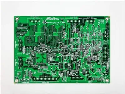
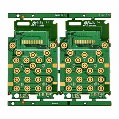
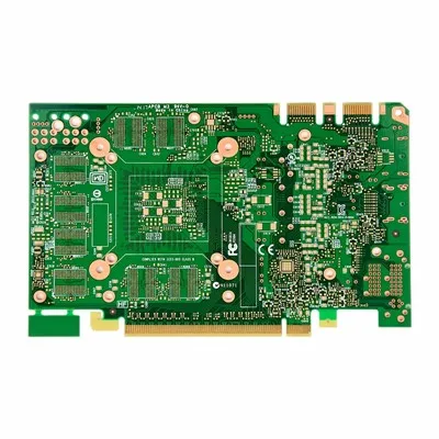
When routing PCBs, the layout of power and ground lines should be the primary consideration. Power lines should be as wide as possible to reduce impedance and heat generation, while ensuring power supply stability. Ground lines need to be complete and continuous, avoiding excessively long loops to reduce noise and electromagnetic interference. In multilayer PCB designs, separate ground and power layers are typically used to improve system immunity and signal stability. For high-current circuits, copper thickness and trace width should be appropriately increased based on current carrying capacity to prevent excessive temperature rise from affecting product reliability. Furthermore, ground lines for analog and digital circuits should be properly separated to avoid mutual interference.
PCB routing also needs to fully consider manufacturing processes and future maintenance needs. Component layout should be as neat and standardized as possible to facilitate SMT placement, soldering, and automated production, while reserving sufficient space for heat dissipation. For components with high heat generation, such as power chips, power modules, and MOSFETs, appropriate amounts of heat-dissipating copper foil or ventilation holes should be added to improve heat dissipation efficiency. Sharp-angle traces, isolated copper foils, and overly dense traces should be avoided during routing to reduce manufacturing defects and electrical risks. Meanwhile, the silkscreen markings should be clear and complete to facilitate later inspection, repair, and debugging. An excellent PCB layout design not only relates to product functionality but also directly impacts equipment stability, production yield, and long-term lifespan.