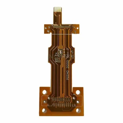

Product Details
High-Density Flex PCB combines high-density interconnect features with flexible substrate materials. It adopts fine-line traces, microvias and compact stack-up structures to achieve dense circuit layout while retaining bending and torsional performance of flex circuits. Compared with conventional multilayer flex PCBs, it supports more components and signal channels within limited space, widely used in compact wearable electronics, camera modules, medical devices and portable communication hardware. Nevertheless, high-density flex PCBs impose higher requirements on fabrication processes. Engineers and buyers need to evaluate trace width-spacing, microvia feasibility, material selection and cost budget to match practical project requirements.

The Growing Challenge of Electronic Miniaturization
Over the past decade, electronic products have evolved dramatically. Customers expect devices to become smaller while simultaneously offering more features.
This trend creates several design challenges:
- More components in limited space
- Increased signal routing requirements
- Higher connector density
- Reduced product thickness
- Complex mechanical layouts
- Weight reduction targets
In many cases, simply increasing layer count is not enough. The available routing area becomes the primary limitation.
High Density Flex PCB technology addresses this issue by utilizing advanced design rules that allow more circuits to be placed within the same physical footprint.

Defining High‑Density Flex PCB Characteristics
The term "high density" does not refer to a single specification. Instead, it describes a combination of design and manufacturing features that increase circuit integration.
Common characteristics include:
Fine Line Routing
Narrow conductor widths and spacing create additional routing channels.
01
Small Via Structures
Reduced via sizes free up valuable board space and improve layout efficiency.
02
Compact Component Placement
Higher density designs support modern miniaturized electronic components.
03
Multilayer Integration
Additional routing layers help accommodate increasingly complex circuits.
04
Precision Manufacturing
Tighter tolerances are required throughout the fabrication process.
Together, these features allow engineers to achieve greater functionality without expanding product size.
05
Applications Driving Demand for High Density Flex PCB
Several industries are adopting high-density flexible circuits to support product innovation.
Wearable Electronics
Smart watches, fitness trackers and health monitoring devices require compact and lightweight circuit solutions.
Medical Devices
Portable diagnostic equipment and patient monitoring systems often demand high functionality within limited space.
Industrial Sensors
Miniaturized sensors and control modules benefit from increased circuit integration.
Communication Equipment
Modern communication devices require dense routing while maintaining signal integrity.
Consumer Electronics
Compact cameras, handheld devices and advanced audio products frequently use high-density flexible circuits.
▲ These applications share a common goal: maximizing performance within increasingly smaller form factors.
Design Considerations During Product Development
Implementing a high-density flexible circuit requires careful planning.
Several factors should be evaluated during the design phase.
Routing Strategy
Efficient routing becomes increasingly important as conductor spacing decreases.
Bend Area Protection
Dense circuitry should be positioned carefully to avoid excessive stress during flexing.
Component Placement
Maintaining sufficient spacing for assembly and reliability remains critical.
Layer Stack-Up Selection
The stack-up must balance routing capacity, flexibility and manufacturing feasibility.
Signal Integrity Requirements
As density increases, signal interaction and impedance control may become more important.
Early collaboration between design teams and manufacturers often reduces development risks and improves production success rates.
Manufacturing Challenges Unique to High Density Flex PCB
While high-density designs provide significant advantages, they also create manufacturing challenges.
▲ Registration Accuracy
Precise alignment is required to ensure circuit features remain within tolerance.
▲ Material Stability
Flexible materials can expand or contract during processing, affecting dimensional accuracy.
▲ Fine Feature Processing
Smaller conductor widths require tighter process control than standard flexible circuits.
▲ Yield Management
As design complexity increases, maintaining consistent production yields becomes more difficult.
▲ Inspection Requirements
Advanced inspection methods are often necessary to verify fine-feature quality.
Manufacturers with experience in high-density flexible circuits typically invest heavily in process control and quality systems to address these challenges.

Reliability Considerations
Many buyers assume that increasing circuit density automatically reduces reliability.
In reality, reliability depends largely on design quality and manufacturing control.
Important reliability factors include:
- Flex cycle performance
- Via integrity
- Material selection
- Thermal stability
- Environmental resistance
- Assembly quality
When properly designed and manufactured, high-density flexible circuits can achieve excellent long-term performance in demanding applications.
Reliability validation should always be performed before transitioning into full production.
Cost‑Saving Advantages of High‑Density Flex PCBs
Although fabrication costs are generally higher than standard flex circuits, overall project economics may improve.
Potential benefits include:
- Smaller product dimensions
- Reduced assembly complexity
- Fewer interconnects
- Lower product weight
- Improved product aesthetics
- Greater functional integration
For many advanced electronic products, these advantages can outweigh the additional PCB manufacturing cost.
The most effective cost analysis considers the complete product rather than focusing only on PCB pricing.
Future Outlook
The trend toward electronic miniaturization is expected to continue across virtually every technology sector.
Several developments are likely to increase demand for High Density Flex PCB solutions:
- Wearable healthcare devices
- Smart industrial sensors
- Portable communication systems
- AI-enabled edge devices
- Advanced consumer electronics
As products continue to shrink while functionality expands, high-density flexible circuits will remain an important enabling technology.
Manufacturers capable of supporting fine-feature processing, multilayer flex construction and reliable volume production will play a critical role in future electronic product development.
FAQ
What is a High Density Flex PCB?
A High Density Flex PCB is a flexible printed circuit designed with fine traces, small vias and compact routing structures to maximize circuit integration within limited space.
How is it different from a standard Flex PCB?
High-density designs utilize tighter design rules and advanced manufacturing processes to support greater functionality in smaller form factors.
Which industries commonly use High Density Flex PCB technology?
Wearable electronics, medical devices, communication equipment, industrial sensors and consumer electronics are among the most common applications.
Does a high-density design increase manufacturing cost?
Yes, fabrication costs are typically higher due to tighter tolerances and more advanced manufacturing requirements.
Hot Tags: high density flex pcb, China high density flex pcb manufacturers, suppliers, factory, circuit flex, flexible pcb led, flexible pcb substrate, flexible printed circuit board, rigid and flexible pcb, rigid flex